Building an MDA/CGA/EGA to VGA Converter - Pt.2
22nd February, 2023
In Part 1, I introduced the GBS8200 - a very cost-effective video converter from China that works well for many games consoles and other home computers, but falls short when used for PCs.
.jpg)
In this Part 2, I will build the Necroware MCE adapter and fully test it.
Stage 1: Building the Necroware MCE-adapter
Necroware has his adapter project up on Github for anyone to create their own. The project provides all the information you should need to be able to construct the board, including the code to be uploaded onto the PLD chip.
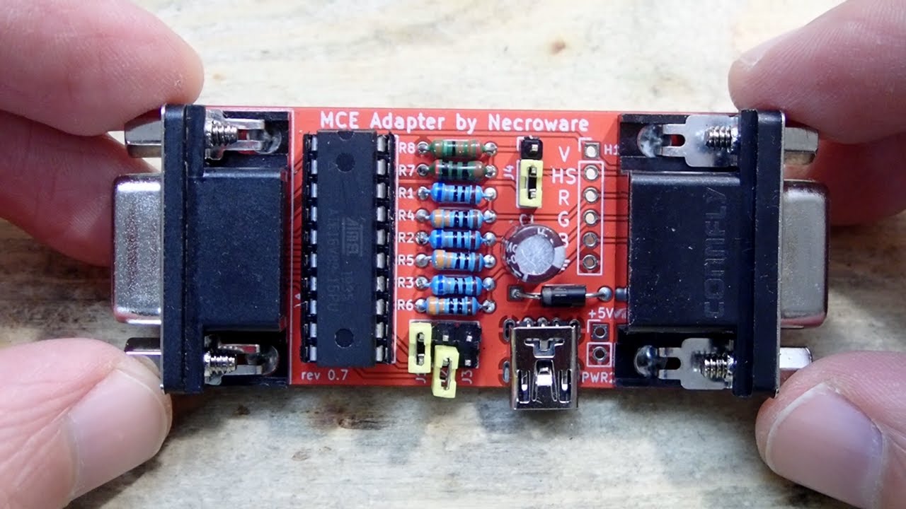
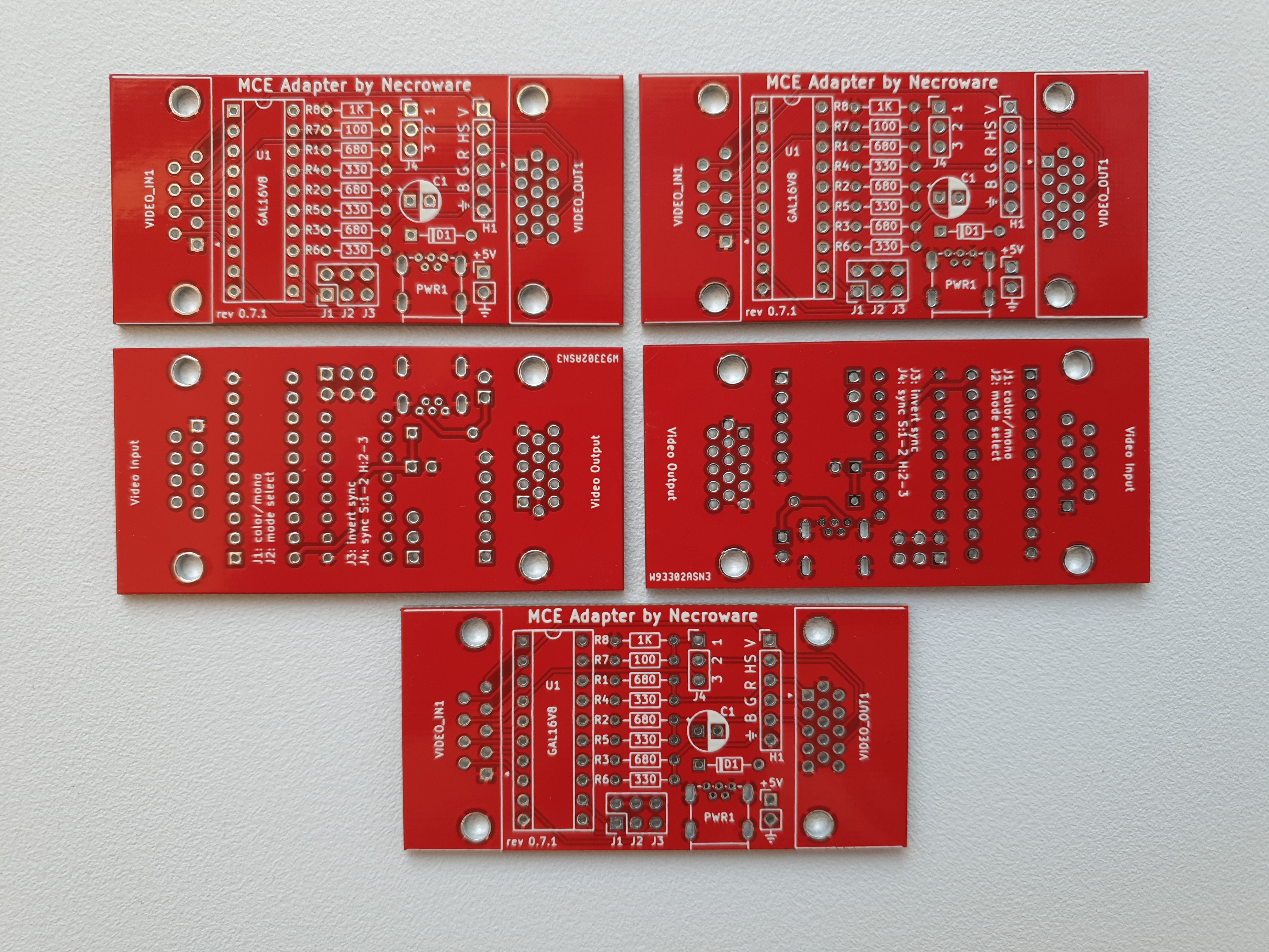
The MCE Adapter by Necroware
As you can see, the adapter has a number of jumpers which I will describe in detail after I have built mine, but in essence they are used to switch between mono and colour, a mode select (depends on mono/colour setting), composite sync signal select (positive/negative), and to switch from composite sync to HV [separate horizontal and vertical] sync.
The Components
To build Necroware's MCE-adapter, here are the components required. I included some more info on what I actually bought and the cost here in the UK:
| Reference | Qty | LCSC | Description | I bought | Cost (£) |
|---|---|---|---|---|---|
| C1 | 1 | C383039 | electrolytic capacitor 220µF | - (already have) | |
| D1 | 1 | C402218 | diode 1N5819 | 1N5819 Schottky Rectifier, 40V, 1A, 2 pins, 550mV | £0.35 |
| H1 | 1 | C492405 | pin header 1x6 | - (already have) | |
| J123 | 1 | C65114 | pin header 2x3 | - (already have) | |
| J4 | 1 | C429954 | pin header 1x3 | - (already have) | |
| PWR1 | 1 | C46398 | USB-B mini port | MOLEX Mini-USB Type B, USB 2.0, 5 ways, through-hole mount, right-angle | £1.83 |
| PWR2 | 1 | C152154 | pin header 1x2 (+5V connector) | - (already have) | |
| R1 R2 R3 | 3 | C58592 | resistor 470 Ohm (or 680 Ohm) | - (already have) | |
| R4 R5 R6 | 3 | C58608 | resistor 330 Ohm | - (already have) | |
| R7 | 1 | C57438 | resistor 100 Ohm | - (already have) | |
| R8 | 1 | C57435 | resistor 1k Ohm | - (already have) | |
| U1 | 1 | C6509 | GAL16V8B (or compatible)* | Atmel ATF16V8B-15PU | £1.05 |
| VIDEO_IN1 | 1 | C141882 | DB9 female connector (MDA/EGA/CGA) | NORCOMP D Sub connector, right-angle, 9 contacts, DE | £1.99 |
| VIDEO_OUT1 | 1 | C75754 | DIB15 female connector (VGA) | MULTICOMP D Sub connector, right-angle, 15 contacts, DA | £1.48 |
*The GAL16V8B from Lattice Semiconductor is no longer manufactured. There are pin-compatible alternative PLDs, such as the Atmel ATF16V8B that work just as well and are readily available for purchase in 2023 - this is the one I used.
The Board
The missing item from the list above is the PCB itself. Necroware's project includes KiCad files that provide all the details required to have the PCB manufactured. Before this project I had never had a PCB manufactured, so I went into this with a fair bit of doubt and trepidation. Having heard of PCBWay, I chose them to manufacture my board. Their website gives you a lot of options which for the uninitiated may seem daunting, but the process was made a lot easier with a bit of help from their support team via the chat window. The only stumbling block I had was that PCBWay won't accept KiCad files - they require Gerber files instead. A member of their support team provided me with a link to a very informative help page describing how to convert KiCad files to Gerber files. This involved me downloading the KiCad software and then exporting the files into Gerber format. The help page handily gave me steps to follow, what board layers were needed, and what options to check/not to check in the KiCad software.
PCBWay require you to upload the Gerber files including the 'drill' files as a single ZIP file. Once uploaded, they review the files to check everything is there for manufacturing. This process takes just 10 minutes or so after you upload the files. Of course, the review they conduct doesn't evaluate whether the circuit's design is functional - it just checks if the minimum of information has been provided for them to etch the circuit board front and rear, that it's of the correct size and has drill hole locations.
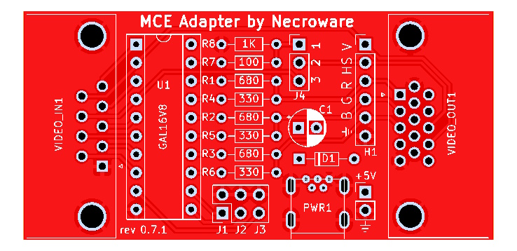
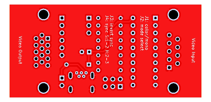
A mock-up from PCBWay of what I'm going to receive: Top and Bottom view
If it all checks out you get an email telling you the review was successful, and proceed to payment. I was told manufacturing would start in about 1 day, and I should expect delivery of my board about 11-13 days later from China. I chose the cheapest delivery option, Global Economy Shipping, to keep costs down, as it's the first time using this service and if I messed up the order somehow it won't break the bank.
The minimum number of boards PCBWay will make is 5, and the cost came to $5 for all five boards plus $4.29 shipping, which I feel is really excellent.
Since this circuit board design is pretty simple, you don't necessarily need to use an external company even for the PCB - you could use a piece of Veroboard or prototyping board, or even create your own using a copper PCB and etch your own tracks, but since Necroware has already done the job of creating a nice board design and the cost was low I felt it made sense to go with this approach.
So all in, the total outlay for the parts came to about £15. I ordered the components that weren't in my parts collection from Farnell Electronics (UK), and these arrived in about 18 hours - great service! Here are all the components I will use once the board arrives:
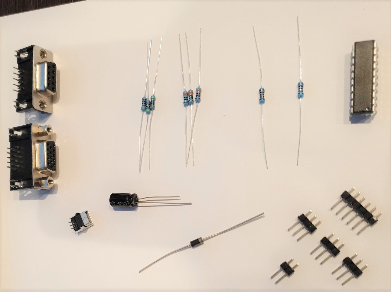
Components ready for the PCB to arrive
Writing the Code to the PLD (GAL)
The Programmable Logic Device (PLD) used here is often referred to as a GAL (Generic Array Logic), though this term is proprietary to the Lattice Semiconductor company that invented it. The common name for this type of IC is a PLD.
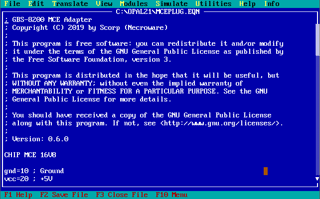
So as of right now, my Atmel PLD chip is empty - we need to put Necroware's little 4 KB program on it. This comes in the form of a .EQN (equation) file, which needs to be compiled and written to the PLD chip. The .EQN file is written in what's called HDL, or Hardware Description Language. It defines the chip type, the meaning of the pins, and the logic of what the output pins values should be, based on the inputs.
A .EQN file needs to be compiled into what's called a "fusemap" before it can be written to the PLD. It's called this because when PLDs were first around, programming them would literally blow fuses inside the chip to create the custom logic - these of course were 'write once', since damage was done internally to produce the logic. Our modern-day PLD here can be overwritten about 100 times. A commonly used fusemap format is JEDEC, which has the file extension .JED.
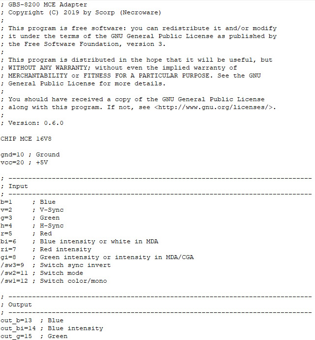
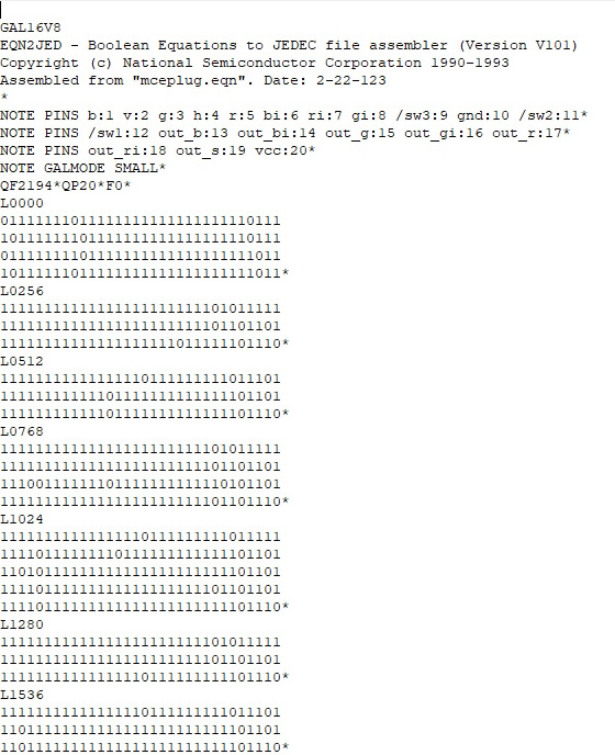
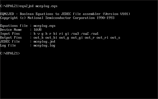
The .EQN file (left), and the compiled .JED file (right)
There are many programs out there that will compile HDL into a fusemap file, including PALWIZ from Bruce Tomlin, VHDL, Verilog, CUPL, WinCUPL, and ABEL. Recommended by Necroware is the DOS utility, EQN2JED.EXE, which is part of a 1993 DOS program called Opal Jr.
The Atmel ATF16V8B PLD I'm using has 16 I/O lines, of which 8 can be outputs. It's ideal for this project, as we need all 8 inputs for Red, Green, Blue, Red Intensity, Green Intensity (or intensity in MDA/CGA), Blue Intensity (or white in MDA), Horizontal Sync, and Vertical Sync. On the output side, we need 7 for Red, Green, Blue, Red Intensity, Green Intensity, Blue Intensity, and combined H+V sync.
OpalJr version 2.1 is used here to create a .JED file from the .EQN file:
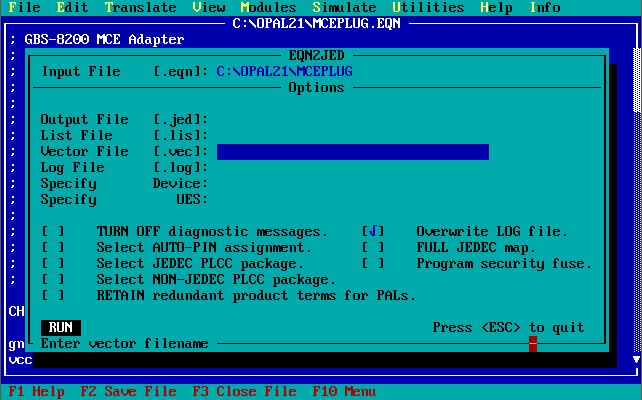
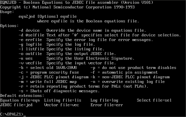
EQN2JED utility, part of the Opal Jr v2.1 application for DOS
We're now ready to write the .JED file to the PLD. This can be done using an IC programmer, like my XP8710 here:
.jpg)
XP8710 USB IC programmer
The XP8710 is just another name for the popular MiniPro TL866A (now replaced with the TL866II-3G, aka T48), and comes with Windows software which can be used to program our Atmel PLD and thousands more devices. The following steps are taken to program the device:
1) Connect the programmer to your PC and run the XP8710 (also known as MiniPro) application.
2) Insert the IC into the programmer and lock the pins in place.
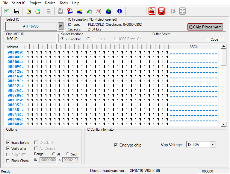
3) Select the correct IC:
4) Open the .JED file (File -> Open) and program the chip:
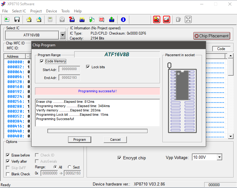
One curiously odd outcome from the programming process is that after writing it still appears to contain only all 1's - usually you're able to see code when reading back from the chip. I wasn't sure if I should have the "Encrypt chip" check box enabled or not, so it's possible that after writing you cannot see the contents - we'll see.
Building the Board
One thing I forgot to put into the components list is a 20-pin DIP socket. If for any reason I need to reprogram the PLD or replace it, it makes sense to socket this chip.
**UPDATE 2nd March 2023 - the boards have arrived!**
Overall, I'm very pleased with how these have come out. The board size is perfect, and has all the traces and drill holes where expected.
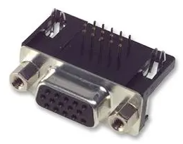 Unfortunately, my early checks tell me the 15-pin D-SUB I purchased has its rows of pins too far apart for the board's design. The component I ordered was described as "MULTICOMP SPC15430 D Sub Connector, Right Angle, HD15, Standard, Receptacle, 15 Contacts, DA, Solder". This appears to have 2.54mm spacing between each of the three rows of pins. The one I need for Necroware's PCB design is 1.98mm spacing. They do sell the correct ones at Farnell Electronics, described as "Amphenol
17EHD015SAA000 - D Sub Connector, High Density, Receptacle, 17EHD, 15 Contacts, DE, Solder Cup", but at £10 for delivery of a single part, I will instead build the circuit with wires soldered to the pins instead. There only needs to be 6 pins connected of the 15, which are Red, Green, Blue, H-Sync (also doubles up as Composite Sync), V-Sync, and GND. I will then secure the VGA port once I have the board inside a plastic case.
Unfortunately, my early checks tell me the 15-pin D-SUB I purchased has its rows of pins too far apart for the board's design. The component I ordered was described as "MULTICOMP SPC15430 D Sub Connector, Right Angle, HD15, Standard, Receptacle, 15 Contacts, DA, Solder". This appears to have 2.54mm spacing between each of the three rows of pins. The one I need for Necroware's PCB design is 1.98mm spacing. They do sell the correct ones at Farnell Electronics, described as "Amphenol
17EHD015SAA000 - D Sub Connector, High Density, Receptacle, 17EHD, 15 Contacts, DE, Solder Cup", but at £10 for delivery of a single part, I will instead build the circuit with wires soldered to the pins instead. There only needs to be 6 pins connected of the 15, which are Red, Green, Blue, H-Sync (also doubles up as Composite Sync), V-Sync, and GND. I will then secure the VGA port once I have the board inside a plastic case.
Completed Assembly
I started with a check over the whole board to ensure we have traces where they need to be (or not). All good, so proceeded with the soldering, starting with the smallest components near the centre of the PCB and working outwards. Here's the finished article:
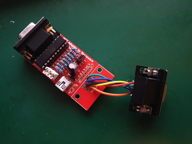
A bit of "iffy" soldering here and there, but everything's in place - a final check before powering up...
In Part 3, I will test the MCE Adapter on some MDA/Hercules, CGA and EGA cards.